

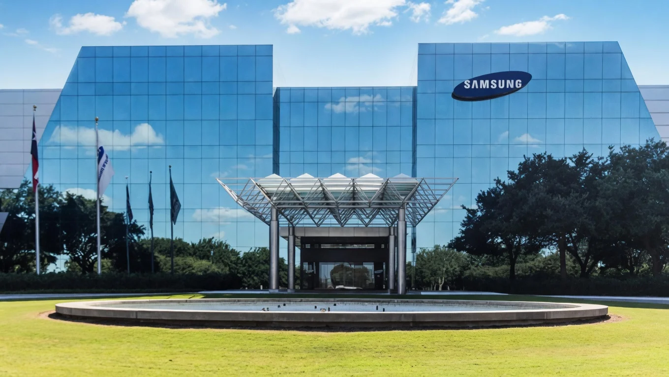
Samsung Electronics, a global leader in advanced semiconductor technology, announced on Friday a significant milestone in the high-bandwidth memory (HBM) sector: the delivery of initial samples of its cutting-edge 12-layer HBM4E memory chips to key clients. This achievement marks a pivotal moment in the competitive landscape of AI memory solutions, showcasing Samsung’s aggressive push for technological leadership. The news reverberated through financial markets, propelling Samsung shares up 5.8% in Seoul trading, while its American rival, Micron Technology, also saw an approximate 2% gain in pre-U.S. market trading, reflecting broadly positive sentiment across the semiconductor industry.
The advanced memory solution, designated HBM4E, represents a substantial leap forward from its predecessor, the HBM4 standard. Benchmarking against the earlier standard, Samsung’s HBM4E offers more than a 20% increase in data throughput and over 30% greater storage capacity. These enhancements are critical for meeting the ever-growing demands of artificial intelligence (AI) and high-performance computing (HPC) workloads, which require immense processing power and rapid data access.
At the core of this innovation lies a sophisticated integration of Samsung’s newest 1c DRAM process node. This represents the company’s sixth-generation 10-nanometer-class DRAM architecture, signifying years of intensive research and development in shrinking transistor sizes and improving efficiency. Complementing this advanced DRAM is a 4-nanometer foundry logic base die, a critical component that facilitates the complex interconnections and control logic for the stacked memory layers. This combination of cutting-edge DRAM manufacturing and advanced foundry capabilities underscores Samsung’s comprehensive strength across the semiconductor value chain.
Accelerated Timeline Underscores Strategic Intent
This latest milestone arrives with remarkable speed, merely three months after Samsung’s February launch of standard HBM4 chip samples. Such an accelerated timeline is a clear indicator of Samsung’s strategic imperative and aggressive pursuit of leadership in the burgeoning AI memory market. The company’s ability to quickly move from initial samples to a more advanced ‘E’ (extended) variant demonstrates its robust R&D capabilities and efficient product development cycles.
In an official statement, Samsung affirmed its commitment to client-centric deployment: "Samsung plans to begin mass production for HBM4E aligned with customer schedules, following initial sample shipments and optimization." This statement highlights the collaborative nature of HBM development, where close cooperation with AI accelerator designers is essential to tailor memory solutions precisely to their architectural requirements.
Among Samsung’s esteemed client roster are industry titans such as Nvidia, AMD, and Google. These companies stand at the forefront of artificial intelligence infrastructure development, driving the insatiable demand for cutting-edge memory solutions. Nvidia, with its dominant position in AI GPUs, and AMD, with its expanding portfolio of AI accelerators, are particularly critical partners, as their future product roadmaps heavily depend on the availability of high-performance, high-capacity HBM. Google, a major developer and deployer of AI models, also relies on advanced memory for its data centers and custom AI chips.
Samsung had previously signaled its intention to ship HBM4E samples during the second quarter of the year (Q2). The company’s announcement confirms that it has successfully met this ambitious commitment, reinforcing its reputation for executing on its technology roadmap.
Understanding High-Bandwidth Memory (HBM) and Its Indispensable Role in AI
To fully appreciate the significance of Samsung’s HBM4E achievement, it’s crucial to understand the technology itself and its pivotal role in the AI revolution. High-Bandwidth Memory (HBM) is a type of 3D-stacked synchronous dynamic random-access memory (SDRAM) that was initially proposed by AMD and Hynix in 2013. Unlike traditional DRAM modules, which are typically planar and communicate over a wide but slower bus, HBM stacks multiple DRAM dies vertically on a base logic die. These layers are interconnected using through-silicon vias (TSVs) and micro-bumps, creating a much wider data pathway and significantly reducing the distance data needs to travel.
The primary advantage of HBM is its ability to overcome the "memory wall" – the bottleneck created by the increasing speed of processors outpacing the speed and bandwidth of conventional memory. For AI and machine learning workloads, which involve processing massive datasets and performing billions of calculations in parallel, traditional memory architectures are simply inadequate. GPUs, the workhorse of AI training and inference, require incredibly fast access to vast amounts of data to keep their thousands of processing cores fully utilized. HBM provides this crucial bandwidth, enabling GPUs to operate at their full potential and significantly accelerating the training of complex neural networks and the execution of sophisticated AI models.
The evolution of HBM technology has been rapid. From HBM1 (introduced with AMD’s Fiji GPU in 2015) to HBM2, HBM2E, HBM3, and now HBM4, each generation has brought improvements in bandwidth, capacity, and power efficiency. HBM3, for instance, offered substantial performance gains over HBM2E, while HBM3E (an enhanced version of HBM3) further pushed the boundaries, becoming the standard for many of today’s most advanced AI accelerators. HBM4 and HBM4E represent the next frontier, promising even greater performance density and efficiency, which are essential as AI models continue to grow in size and complexity. The transition to a 12-layer stack in HBM4E, up from typical 8-layer or 12-layer configurations in previous generations, directly contributes to the increased capacity and density required for future AI systems.
Implications for Micron and the Competitive Landscape
Micron Technology, based in the United States, stands as the primary American rival to South Korea’s Samsung and SK Hynix in the highly specialized and competitive field of high-bandwidth memory production. While Samsung’s latest announcement could be perceived as a direct competitive move, the current market dynamics tell a more nuanced and complex story.
Micron has previously made public statements indicating that its entire HBM4 production capacity is already fully allocated and pre-sold through 2026. This means that, at least for the immediate future, Samsung’s advancement with HBM4E is unlikely to directly erode Micron’s existing market position or revenue streams. The insatiable demand for HBM, driven by the explosive growth of AI, has created a situation where supply severely lags behind demand, allowing all major players to secure orders well in advance.
The overall HBM market is experiencing unprecedented growth. According to projections by BNP Paribas, the market is expected to more than double in 2025, reaching approximately $76 billion. This staggering growth trajectory is anticipated to continue, with the market climbing further to an estimated $156 billion by 2027. Such robust and sustained expansion provides ample opportunity for all three major manufacturers – SK Hynix, Samsung, and Micron – to prosper and capture significant revenue, even as they intensely compete for technological leadership and market share.
Despite Samsung’s rapid progress, SK Hynix has historically held a dominant position in the HBM market. As of late 2025, data from Counterpoint Research indicated that SK Hynix controlled a significant 57% of the global HBM revenue share. Samsung accounted for 22%, while Micron represented 21%. These figures highlight SK Hynix’s early lead and strong execution, particularly in securing key partnerships for HBM3 and HBM3E. However, Samsung’s aggressive advancements with HBM4 and HBM4E suggest a concerted effort to narrow this competitive gap, and perhaps even challenge for the top spot in future generations. The speed with which Samsung has brought its HBM4E samples to market is indeed more rapid than many industry observers had anticipated, signaling a potentially significant shift in market dynamics.
Broader Market Context and AI Demand
The broader semiconductor sector has experienced substantial momentum, largely fueled by the AI boom. Micron, for example, has seen its stock perform exceptionally well, reflecting investor confidence in its position within the AI memory ecosystem. Samsung’s HBM4E debut, while a major competitive statement, appears unlikely to immediately disrupt this positive trajectory for Micron or the industry as a whole, primarily due to persistent supply constraints. The demand for advanced memory is so high that even with new entrants or accelerated product launches, the market can absorb all available supply.
SK Hynix maintains its position as the HBM market leader, having forged strong relationships with key AI GPU manufacturers. However, Samsung’s current trajectory suggests it is not only narrowing the competitive distance but doing so at a pace that has surprised many industry analysts. This intensified competition is ultimately beneficial for customers, driving innovation, improving performance, and potentially leading to more competitive pricing in the long term.
Amidst this flurry of memory innovation, Nvidia, one of the largest consumers of HBM chips, also traded up 0.78% on Friday. This upward movement reflects the generally positive sentiment across the sector and underscores the critical importance of HBM availability for the continued growth and development of the AI industry. The performance of AI companies is inextricably linked to the advancements in underlying hardware, particularly memory, which acts as the lifeblood of data processing.
Samsung’s HBM4E incorporates the company’s most sophisticated DRAM technology node to date. This technological superiority, combined with the advanced packaging of a 12-layer stack and a 4-nanometer logic base die, positions the product strategically for the rigorous demands of upcoming AI computing platforms. These future platforms will require not only higher bandwidth and capacity but also improved power efficiency, as data centers grapple with increasing energy consumption. The ability to integrate more memory into a smaller footprint while maintaining high performance and reducing power draw is a key differentiator that Samsung aims to leverage.
The Future Outlook and Mass Production
The delivery of initial samples is a critical step, but the ultimate success of HBM4E hinges on its seamless transition to mass production. Samsung’s statement regarding aligning mass production with customer schedules highlights the intricate coordination required between memory manufacturers and their clients. The process involves extensive testing, validation, and optimization to ensure reliability, yield rates, and compatibility with the diverse architectures of AI accelerators.
The capital expenditure required for HBM manufacturing is immense, necessitating significant investments in advanced fabrication facilities (fabs), packaging technologies, and R&D. The ability to achieve high yield rates for such complex stacked structures is paramount for profitability. As the HBM market continues its rapid expansion, the ability of companies like Samsung, SK Hynix, and Micron to scale production efficiently and maintain quality will be crucial determinants of their long-term success.
Looking ahead, the demand for HBM is expected to intensify further as AI models become even larger and more sophisticated. The advent of multi-modal AI, edge AI, and new computational paradigms will continue to push the boundaries of memory technology. Samsung’s early delivery of HBM4E samples positions it favorably to capture a significant share of this future growth, potentially influencing the design and capabilities of the next generation of AI supercomputers and data centers. The race for AI memory leadership is far from over, but Samsung has just fired a significant volley, demonstrating its formidable capabilities and unwavering commitment to advancing the frontiers of computing.